PCB
In the world of electronics, two acronyms are frequently used: PCB and PCBA. Both play pivotal roles in modern technology, but they serve different functions and are often misunderstood. Whether you’re a hobbyist, engineer, or involved in electronics manufacturing, understanding the distinction between Printed Circuit Boards (PCB) and Printed Circuit Board Assemblies (PCBA) is essential. In this article, we’ll explore the meaning of PCBA, the assembly process, and the differences between PCB and PCBA to help clarify their roles in the electronics industry.
What’s the Meaning of PCBA?
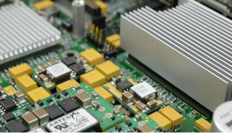
PCBA stands for Printed Circuit Board Assembly, which refers to the entire process of assembling electronic components onto a bare PCB. A PCBA is essentially a finished, functional circuit board that has all its components, like resistors, capacitors, and integrated circuits (ICs), soldered into place. In contrast, a PCB refers to the bare board, which is just a platform with copper traces but no components installed yet.
In summary, while a PCB is the physical board without any components, a PCBA is a complete and functional electronic product that can perform its designated tasks.
The Process of PCB Assembly
PCB assembly (PCBA) involves multiple steps to transform a blank PCB into a functional board capable of driving an electronic system. Let’s break down the process:
Solder Paste Application: The process begins with applying solder paste to the PCB. A stencil is used to apply this paste only to specific areas where electronic components will be placed. The solder paste consists of tiny metal balls mixed with flux to hold components in place during the assembly.
Component Placement: After applying the solder paste, the board moves into a pick-and-place machine. This machine places the surface mount devices (SMDs) such as resistors, capacitors, and ICs onto the designated spots. The components are positioned automatically with extreme precision based on the PCB design file.
Reflow Soldering: After placing the components, the board is passed through a reflow oven. This oven heats the board to a temperature that melts the solder paste, creating permanent electrical connections between the PCB and the components. As the board exits the oven and cools down, the solder solidifies, securing the components in place.
Inspection and Testing: Once soldering is complete, the PCB goes through a quality control inspection. Automated optical inspection (AOI) systems scan the board for errors, such as misplaced components or solder bridges. For more complex boards, X-ray inspection may be used to examine hidden solder joints, particularly for ball grid arrays (BGAs). After inspection, the PCBA is tested to ensure it works as intended.
Thru-Hole Component Assembly (Optional): Some assemblies may require through-hole components. In this case, the components are manually inserted into holes drilled into the PCB and then soldered, either manually or using wave soldering techniques.
Final Inspection and Functional Testing: After all components are in place and the board is assembled, the final step is to conduct functional testing to verify that the assembled PCBA works as intended. This ensures that all circuits function correctly under real-world conditions.
PCB vs. PCBA: What’s the Difference Between Them?
While the terms PCB and PCBA are often used interchangeably, they refer to different stages in the manufacturing process. Here’s a closer look at each:
What is PCB?
A Printed Circuit Board (PCB) is a flat, insulated board made from fiberglass, composite epoxy, or other laminate materials. It has conductive pathways, or copper traces, etched onto it, which electrically connect different components to each other. However, a PCB on its own is just a bare board. It contains no electronic components and cannot perform any electronic functions. It serves as the skeleton or foundation of electronic devices, providing structure and routing for electrical signals.
PCBs can have various layers depending on the complexity of the design. For instance, there are single-layer, double-layer, and multi-layer PCBs, where multiple layers of conductive traces can be stacked to accommodate more complex circuits.
What’s the Difference Between PCB and PCBA?
PCB (Printed Circuit Board): A PCB is the raw, unfinished circuit board without any electronic components. It provides the physical framework for placing components and establishes electrical pathways between them. However, it is non-functional on its own.
PCBA (Printed Circuit Board Assembly): A PCBA, on the other hand, is a finished product where all the components, such as resistors, capacitors, transistors, ICs, and other electronic parts, are mounted and soldered onto the PCB. It is a fully functional assembly that can be installed in an electronic device to perform its intended tasks.
The primary difference between PCB and PCBA is that PCBs are incomplete and non-functional, while PCBAs are fully assembled, functional units that are ready for integration into a final product.
Conclusion
In summary, understanding the distinction between PCB and PCBA is crucial in the electronics industry. A PCB refers to a bare circuit board that serves as the foundation for assembling electronic components, while a PCBA is the complete assembly of the board with all the necessary components soldered in place. The assembly process of a PCBA involves various steps, from solder paste application to component placement, reflow soldering, inspection, and testing.
While PCBs serve as a physical structure, PCBAs provide the functionality needed to power electronic devices. Without both, modern electronics like smartphones, computers, and appliances would not be possible. For manufacturers, engineers, and designers, knowing the difference and the role each plays is key to producing high-quality, reliable electronics products.